Firstly I would like to say that the following project is an initial example for who wishes start a work with VHDL, after read this example you will be able to simulate your first digital design in vhdl.
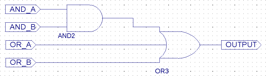
The circuit below represents two logical gates “AND” and “OR”, and their corresponding input AND_A, AND_B, OR_A and OR_B. Note that this circuit was generated automatic through the RTL generation, for this case it was generated by Xilinx ISE Tool.
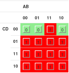
Below is possible to see the truth table for the circuit above.

In the following image is possible see the Karnaugh map for the same circuit.
LIBRARY ieee;
USE ieee.std_logic_1164.ALL;
USE ieee.numeric_std.ALL;
LIBRARY UNISIM;
USE UNISIM.Vcomponents.ALL;
ENTITY teste_and_teste_and_sch_tb IS
END teste_and_teste_and_sch_tb;
ARCHITECTURE behavioral OF teste_and_teste_and_sch_tb IS
COMPONENT teste_and
PORT( AND_A : IN STD_LOGIC;
AND_B : IN STD_LOGIC;
OR_A : IN STD_LOGIC;
OR_B : IN STD_LOGIC;
OUTPUT : OUT STD_LOGIC);
END COMPONENT;
SIGNAL AND_A : STD_LOGIC;
SIGNAL AND_B : STD_LOGIC;
SIGNAL OR_A : STD_LOGIC;
SIGNAL OR_B : STD_LOGIC;
SIGNAL OUTPUT: STD_LOGIC;
BEGIN
UUT: teste_and PORT MAP(
AND_A => AND_A,
AND_B => AND_B,
OR_A => OR_A,
OR_B => OR_B,
OUTPUT => OUTPUT
);
-- *** Test Bench - User Defined Section ***
tb : PROCESS
BEGIN
WAIT FOR 10 NS; -- will wait 10 ns
AND_A <= '0';
AND_B <= '0';
OR_A <= '0';
OR_B <= '0';
WAIT FOR 10 NS; -- will wait 10 ns
AND_A <= '0';
AND_B <= '0';
OR_A <= '0';
OR_B <= '1';
WAIT FOR 10 NS; -- will wait 10 ns
AND_A <= '0';
AND_B <= '0';
OR_A <= '1';
OR_B <= '0';
WAIT FOR 10 NS; -- will wait 10 ns
AND_A <= '0';
AND_B <= '0';
OR_A <= '1';
OR_B <= '1';
WAIT FOR 10 NS; -- will wait 10 ns
AND_A <= '0';
AND_B <= '1';
OR_A <= '0';
OR_B <= '0';
WAIT FOR 10 NS; -- will wait 10 ns
AND_A <= '0';
AND_B <= '1';
OR_A <= '0';
OR_B <= '1';
WAIT FOR 10 NS; -- will wait 10 ns
AND_A <= '0';
AND_B <= '1';
OR_A <= '1';
OR_B <= '0';
WAIT FOR 10 NS; -- will wait 10 ns
AND_A <= '0';
AND_B <= '1';
OR_A <= '1';
OR_B <= '1';
WAIT FOR 10 NS; -- will wait 10 ns
AND_A <= '1';
AND_B <= '0';
OR_A <= '0';
OR_B <= '0';
WAIT FOR 10 NS; -- will wait 10 ns
AND_A <= '1';
AND_B <= '0';
OR_A <= '0';
OR_B <= '1';
WAIT FOR 10 NS; -- will wait 10 ns
AND_A <= '1';
AND_B <= '0';
OR_A <= '1';
OR_B <= '0';
WAIT FOR 10 NS; -- will wait 10 ns
AND_A <= '1';
AND_B <= '0';
OR_A <= '1';
OR_B <= '1';
WAIT FOR 10 NS; -- will wait 10 ns
AND_A <= '1';
AND_B <= '1';
OR_A <= '0';
OR_B <= '0';
WAIT FOR 10 NS; -- will wait 10 ns
AND_A <= '1';
AND_B <= '1';
OR_A <= '0';
OR_B <= '1';
WAIT FOR 10 NS; -- will wait 10 ns
AND_A <= '1';
AND_B <= '1';
OR_A <= '1';
OR_B <= '0';
WAIT FOR 10 NS; -- will wait 10 ns
AND_A <= '1';
AND_B <= '1';
OR_A <= '1';
OR_B <= '1';
END PROCESS;
-- *** End Test Bench - User Defined Section ***
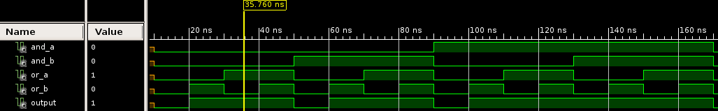
END;The image below shows the time diagram for the test bench described above, here we can all entries and their corresponding outputs.
I hope you had fun here!
